28+ Pcb Layout Design Gambar Minimalis
Poin pembahasan 28+ Pcb Layout Design Gambar Minimalis adalah :
28+ Pcb Layout Design Gambar Minimalis. Dalam dunia skema pcb mungkin Anda pernah mendengar dengan yang namanya kumpulan skema pcb. Komponen dasar skema pcb beserta fungsi dan simbolnya yang harus kamu ketahui, Simak ulasan terkait skema pcb dengan artikel 28+ Pcb Layout Design Gambar Minimalis berikut ini

PCB Layout Fast Forward DDR3 Memory Layout YouTube Sumber : www.youtube.com

PCB Layout Sumber : www.ancorlabs.org

PCB Placement and Routing Mentor Graphics Sumber : www.mentor.com

Watch routing PCB Layout with DDR3 High Speed Interfaces Sumber : www.youtube.com

simple pcb layout design tooling design BGA assembly Sumber : www.ourpcbte.com

Best of Free 10 PCB Design SoftwareElectronics Project Circuts Sumber : electroneecs-project.blogspot.com

PCB Layout Design Software Zuken USA Sumber : us.zuken.com

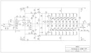
PCB Layout Design Electronic Circuit Sumber : www.elcircuit.com

microcontroller PCB layout questions for MCU breakout Sumber : electronics.stackexchange.com

Online Advanced PCB Layout Course by Motherboard Designer Sumber : www.fedevel.com

How to do a PCB layout review Fully Charged Archives Sumber : e2e.ti.com

PCB Layout Design Software Zuken USA Sumber : us.zuken.com
1Make important nodes accessible., 2Give space between components., 3Place components with the same orientation., 4Print the layout to see if components" sizes match., 5Exchange wiring directions between layers., 6Select the width of lines depending on current., 7Know the specifications of the manufacturer., 8Avoid 90 angles with traces., 1Allegro Cadence. Allegro Cadence is a professional PCB design software that has a wide set of features. ..., 2PADS. Among the more affordable solutions, PADS is one of the best PCB design software. ..., 3OrCAD. ..., 4Kicad. ..., 5Altium Designer (PROTEL) ..., 6Eagle. ..., 7EasyEda. ..., 8DesignSpark PCB., download software pcb layout, pcb design software, pcb design online, pcb designer, eagle pcb, simulator pcb, eagle pcb drawing, what is eagle pcb software,

PCB Design Tips General Electronics Tutorial YouTube Sumber : www.youtube.com

Professional High Tg FR4 Electronic Circuit Board PCB Sumber : www.custompcbboards.com

Schematic Simulation PCB Design and Solid Modeling YouTube Sumber : www.youtube.com
1Make important nodes accessible., 2Give space between components., 3Place components with the same orientation., 4Print the layout to see if components" sizes match., 5Exchange wiring directions between layers., 6Select the width of lines depending on current., 7Know the specifications of the manufacturer., 8Avoid 90 angles with traces., 1Allegro Cadence. Allegro Cadence is a professional PCB design software that has a wide set of features. ..., 2PADS. Among the more affordable solutions, PADS is one of the best PCB design software. ..., 3OrCAD. ..., 4Kicad. ..., 5Altium Designer (PROTEL) ..., 6Eagle. ..., 7EasyEda. ..., 8DesignSpark PCB., download software pcb layout, pcb design software, pcb design online, pcb designer, eagle pcb, simulator pcb, eagle pcb drawing, what is eagle pcb software,
28+ Pcb Layout Design Gambar Minimalis. Dalam dunia skema pcb mungkin Anda pernah mendengar dengan yang namanya kumpulan skema pcb. Komponen dasar skema pcb beserta fungsi dan simbolnya yang harus kamu ketahui, Simak ulasan terkait skema pcb dengan artikel 28+ Pcb Layout Design Gambar Minimalis berikut ini
PCB Layout Fast Forward DDR3 Memory Layout YouTube Sumber : www.youtube.com
PCB Layout DipTrace
PCB Layout Sumber : www.ancorlabs.org
PCB Layout Design Electronic Circuit
PCB Layout is a high level engineering tool for board design featuring smart manual routing of high speed and differential signals shape based autorouter advanced verification and wide import export capabilities Design requirements are defined by net classes class to class rules and detailed settings by object types for each class or layer
PCB Placement and Routing Mentor Graphics Sumber : www.mentor.com
How to Design a PCB Layout Circuit Basics
PCB Layout and Design We use different PCB design softwares to meet your needs Altium Designer Cadence Orcad or Allegro Eagle KiCAD which provides very high level PCB design files and full 3D CAD design output capabilities
Watch routing PCB Layout with DDR3 High Speed Interfaces Sumber : www.youtube.com
10 Free PCB Design Software ElectroSchematics com
PCB Layout Design Upload Schematic Upload We accept EAGLE KiCad OrCAD or Altium schematic files Additional files will be requested in the next step PCB Manufacturing Click the button below to begin an online quote with instant pricing via our partner shop Royal Circuits
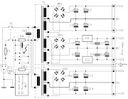
simple pcb layout design tooling design BGA assembly Sumber : www.ourpcbte.com
PCBLayout com
Best of Free 10 PCB Design SoftwareElectronics Project Circuts Sumber : electroneecs-project.blogspot.com
Design Services PCB Layout PCB Design Industrial Design
PCB Layout Design See this ultra high power amplifier video complete tutorial and how to make PCB IC Components Suppliers EasyEDA PCB Design Software Electronic Circuit Design Free Online Gerber Viewer JLCPCB PCB Prototype Manufacturer Electronic Components Store Reliable PCB Prototype Supplier Power Amplifier 2SC5200 2SA1943
PCB Layout Design Software Zuken USA Sumber : us.zuken.com
PCB Layout Design Electronic Circuit Sumber : www.elcircuit.com
microcontroller PCB layout questions for MCU breakout Sumber : electronics.stackexchange.com
Online Advanced PCB Layout Course by Motherboard Designer Sumber : www.fedevel.com
How to do a PCB layout review Fully Charged Archives Sumber : e2e.ti.com
PCB Layout Design Software Zuken USA Sumber : us.zuken.com
1Make important nodes accessible., 2Give space between components., 3Place components with the same orientation., 4Print the layout to see if components" sizes match., 5Exchange wiring directions between layers., 6Select the width of lines depending on current., 7Know the specifications of the manufacturer., 8Avoid 90 angles with traces., 1Allegro Cadence. Allegro Cadence is a professional PCB design software that has a wide set of features. ..., 2PADS. Among the more affordable solutions, PADS is one of the best PCB design software. ..., 3OrCAD. ..., 4Kicad. ..., 5Altium Designer (PROTEL) ..., 6Eagle. ..., 7EasyEda. ..., 8DesignSpark PCB., download software pcb layout, pcb design software, pcb design online, pcb designer, eagle pcb, simulator pcb, eagle pcb drawing, what is eagle pcb software,
PCB Design Tips General Electronics Tutorial YouTube Sumber : www.youtube.com
Professional High Tg FR4 Electronic Circuit Board PCB Sumber : www.custompcbboards.com
Schematic Simulation PCB Design and Solid Modeling YouTube Sumber : www.youtube.com


0 Comments